Energy Loss In CdTe Solar Cells
Tandem and III-V Solar Cells
Tandem Solar Cells
Conventional solar cells contain a single semiconductor layer, most commonly doped silicon (Si). New advancements in solar cell design called tandem PV devices, however, are solar cells that consist of multiple thin layers of different crystalline semiconductors stacked on top of each other. These semiconductors are made into n-type and p-type materials through the process of doping to increase the possible number of minority carriers available, heightening the electricity generation of a cell. The space between an n-type and a p-type semiconductor wafer is known as a junction; tandem devices containing two or more semiconductor junctions are consequently known as multi-junction solar cells.
Vocab
Minority Carrier
-
An electron that has received energy from a photon, entering an excited state and becoming free from the shell of its atom.
Incident Light
-
The light that hits a solar cell during a period of observation.
Substrate
-
A material that other compounds grow on, almost like a “growing platform."
-
In the case of photovoltaics, semiconductor compounds solidify on a substrate.
Tandem PV devices are far more efficient than Si cells because of the special relationship between their semiconductor layers: each material has a higher bandgap than the material below it, with the top layer having the highest bandgap and the bottom layer having the lowest. When photons hit the top semiconductor layer of a tandem cell, high energy light is absorbed, while lower energy photons that fail to reach the material’s bandgap pass through to the next layer. This filtering process repeats for each layer, and enables lower energy photons to reach semiconductors that will absorb and make use of them.
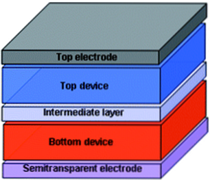
A three-dimensional outline for a single-junction tandem cell.
Image: Royal Society of Chemistry
In one-junction cells, photons that fail to meet the semiconductor’s bandgap energy pass through the material, and their energy is never used. By greatly increasing the number of photons that can be utilized by a solar cell, tandem devices access energy that would otherwise be wasted. Tandem devices therefore generate far more electricity than traditional one-junction Si cells from the same amount of incident light. As you might expect, when compared to a device with similar semiconductor materials, a device with more junctions will be more efficient, as it will filter light more precisely and contain multiple semiconductors with diverse bandgaps.
III-V Solar Cells
III-V solar cells—known by researchers worldwide for their high flexibility and efficiency—are tandem PV devices whose semiconductor layers are made of alloys consisting of elements from groups 3 and 5 of the periodic table. Though not always, III-Vs commonly consist of GaAs (Gallium arsenide), a semiconductor that absorbs light roughly 100x more effectively than the Si in traditional solar cells. Many III-Vs can consequently be made 100x thinner than Si cells, enabling them to be far more flexible. These devices are so flexible, in fact, that they can be stored in rolls for easy portability and installation, and can be laminated onto uneven surfaces, allowing them to be utilized in a wide variety of interesting and useful situations.
III-Vs are currently the most efficient PV devices ever created. In 2020, the National Renewable Energy Laboratory (NREL) built a 6-junction III-V solar cell with an efficiency of 47.1% under 143 suns concentration, the highest recorded efficiency in the history of PV devices. This dwarfs the efficiency of standard commercial Si cells, which average between 20-22%. The incredible efficiency and flexibility of III-V solar cells make them the most electrically viable and versatile type of PV tech there is, but their high manufacturing cost prevents them from reaching commercial practicality.
To manufacture a III-V PV device is a complicated process that can be done in a number of different ways, most of which involve some kind of vapor deposition. Vapor deposition is the process of releasing elements in a gaseous form into a controlled space and waiting for them to settle onto a metallic substrate. Once subjected to certain temperature conditions, these elements solidify into the electricity-conducting, photovoltaic crystals that are the most important layers of a III-V cell. Organometallic Vapor Phase Epitaxy (OMVPE) is the most widely commercialized manufacturing process for III-Vs. A technique used to manufacture all kinds of semiconductor-based devices from LEDs to optoelectronic integrated circuits to solar cells, OMVPE is extremely favorable to manufacturers in part because the technology is used for many different products, making it relatively cheap to obtain.
An interesting vapor deposition manufacturing technique known as Hydride Vapor Phase Epitaxy, or HVPE, is still laboratory-scale, but could one day become mainstream due to its significant increase in production speed and material efficiency compared to the current commercial manufacturing technologies. To perform HVPE, first a plate of pure GaAs is placed in an HVPE reactor, a machine that contains an incredibly controlled environment, to serve as a substrate. Special gases known as precursors are then released into the reactor in a specific order, and as a result of the reactor’s controlled environment—namely its high temperature—they fuse to form semiconductor compounds. These compounds settle one by one on the GaAs plate.
Once the precursors have yielded semiconductors on top of the substrate, the core of the III-V device is ready to be made into a working solar cell. This is done through a process called metallization, where the crystalline layers formed by vapor deposition are outfitted with all the extra materials necessary to become a fully functional device. An example of this would be the application of metal contacts to the front and back of the crystals. Made from thin strips of highly conductive metals, these contacts attract freed electrons from the photon-absorbing layers of a cell and transport them away from the cell for human use as electricity. Attaching an anti-reflective glass coating to the outside of a solar cell also falls under metallization, as it is a part of the post-substrate-growth processing of a cell.

A III-V solar cell with its incredible flexibility on display.
Image: Dennis Schroeder/NREL
Because III-V cells are so expensive to manufacture, they are currently used only in specialized high tech applications such as satellites and military drones. There are three aspects of the III-V manufacturing process that drive the cost. First and foremost is the cost of the substrate, which is made out of pure GaAs to ensure the HVPE process functions properly. An average wafer of GaAs substrate used for HVPE is only 6 inches in diameter and 600 microns thick, but costs around $90, driving up the price to produce III-Vs. This cost depends on material availability and wafer manufacturing, making it difficult to lower, and raises the materials cost of III-V cells far higher than that of most other solar cells. In an effort to reduce their need for pure GaAs, scientists have developed ways to separate a substrate from completed III-V devices, allowing them to reuse it multiple times. This has no adverse effects on III-V devices, as GaAs substrates are not an operational part of a finished cell once the semiconductor compounds have been established, and are actually a detriment in that they restrict the flexibility of III-V cells.
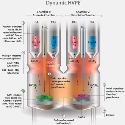
An illustration of the dual-chamber D-HVPE reactor at NREL.
Image: National Renewable Energy Laboratory
One technique used to separate a substrate from a device is known as controlled spalling, which involves infusing a fracture between the III-V device and the substrate to forcefully separate the material. As of now, however, controlled spalling is only laboratory-scale, and is not yet a commercial reality. On the other hand, Epitaxial Liftoff (ELO) is a more widely-used, commercially practical way to reuse a substrate. ELO utilizes a special detachable release layer, generally made out of AlGaAs (Aluminum gallium arsenide), to serve as a thin cover for the substrate of a solar cell. Once vapor phase epitaxy is completed, the AlGaAs strip and the newly formed photo-absorbing layers on top of it are separated from the substrate, enabling it to be used again.
Another economic barrier posed by the III-V manufacturing process is the cost of precursors. Only a small percentage of precursor compounds—roughly 10% for commercial OMVPE processes, though this number is dependent on the reactor and technology in use—end up fusing to form semiconductor materials, so a large quantity of these gases is required to manufacture III-V cells. Current commercialized manufacturing techniques also take hours to grow individual cells, during which precursors must be released continually into the reactor. The sheer volume of precursors required to manufacture a III-V solar cell is a costly investment. The significantly lower manufacturing time and required precursor levels of HVPE consequently indicate the technology’s potential as a commercial alternative.
Finally, the cost of metallization serves as a hurdle for III-V manufacturers, as the process of outfitting III-Vs with various materials, some of which increase the efficiency of a cell depending on their quality, is expensive. To lower the cost of metallization, the process must become more simple and utilize cheaper, more accessible materials. Aside from manufacturing costs, the physical attachment of III-V devices to modules such as satellites adds a whole other set of expenses to the technology that serve as a further economic deterrent for commercial use.
Researchers today, such as those in NREL's Low-Cost III-V Solar Cells lab, are working to reduce the manufacturing cost and time of III-V devices to increase their appeal and practicality. The lab recently developed the process of Dynamic Hydride Vapor Phase Epitaxy (D-HVPE), an improvement to the lab-scale HVPE process. D-HVPE enables the use of cheaper precursor compounds with efficiencies as high as 70-80%, a major contrast to the previously discussed 10% efficiency of OMVPE precursors, speeding up the manufacturing time of III-V devices by a factor of up to 50 or 60. This means that with D-HVPE, III-V solar cell production is not measured in the traditional cells per hour but in cells per minute, increasing cell production while lowering materials costs. The lab’s next goal is to upscale the D-HVPE process for commercial use.
References
Breiland, William G, et al. “Organometallic Vapor Phase Epitaxy (OMVPE).” ResearchGate, 12 Oct. 1998, www.researchgate.net/publication/222302960_Organometallic_vapor_phase_epitaxy_OMVPE.
Tatavarti, Rao, et al. “Lightweight, Low-Cost InGaP/GaAs Dual-Junction Solar Cells on 4’ Epitaxial Liftoff (ELO) Wafers.” ResearchGate, June 2009, www.researchgate.net/figure/ELO-solar-cell-process-flow_fig2_251918998.
Special thanks to the Low-Cost III-V Solar Cells Lab at NREL